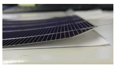
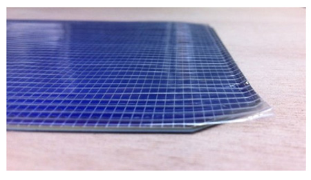
The cells experience some stress during its fabrication and the module fabrication process. In the extreme case, this causes cracks and/or cell breakage. The reasons behind cell breakage in a module are complex. While it can happen at any point between ingot growth and lamination, breakage can be avoided if appropri- ate wafer material is selected and stress on the wafer is reduced throughout the process. SWCT exerts less stress on the wafer than standard soldering technologies thanks to the reduced tempera- ture process (<160°C) and the flexibility of the multiple thin 200 μm wires as opposed to the three stiffer ribbons of 1-2 mm in width. The bow of cell after interconnection is an excellent signature of this stress as shown in Figure 8 where similar monocrystalline cell was interconnected with ribbon and SWCT.

Cell stress
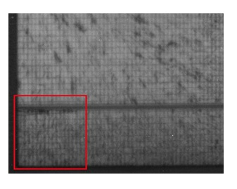
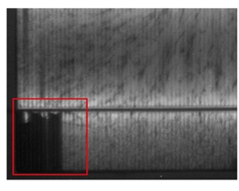
In the event of cell breakage, SWCT can decrease another po- tential negative effect. Earlier studies, such as that of Sander et al. [6], showed that ribbon interconnections were the root cause of cracks and that cracks parallel to the ribbon would make the cell inactive. Cell breakage is reproduced here in Figure 9 to illustrate the be- havior of SWCT compared to ribbon technology. Two cells were deliberately broken in a similar procedure along the length of the busbar (red square). One cell was interconnected with SWCT and the other cell was soldered with two ribbons. This experiment demonstrated that the cells con- nected with SWCT were still completely active, even though the cell was broken. In contrast, the cell connected with ribbons had a completely in- active area (dark area in red square).