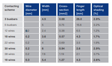
Achieving the highest possible level of efficiency out of a given solar cell power class is the ulti- mate aim of solar module technology. However, the Si solar cells are brittle and are subjected to degradation in humid and oxidizing environment, therefore they need to be protected to resist out- door conditions such as rain, hail, damp, wind and snow. The protection is usually achieved by embedding the cells between encapsulation lay- ers that are laminated between two glasses or glass-backsheet. This gives rise to optical losses compared with the bare cell measurements, due to light reflection and parasitic absorption. In ad- dition, since the photo-generated current needs to be transported from one cell to the other and then out of the module, electrical losses occur. The most reliable, proven and common tech- nique used today is ribbon soldering. Here, we will point out a few advantages of the SWCT compared to this mainstream technology. Electrical loss in solar modules. The front side of conventional crystalline silicon solar cells has fingers and busbars. Fingers col- lect current generated in the cell to the busbars. From these busbars, current flows to copper ribbon that is soldered to each busbar. These ribbons make it possible to transport the photo- generated current out of the solar cell area to the next solar cells. This, in turn, forms a string and the strings are connected in series to form a module. A decade ago, all PV modules were built with solar cells containing two busbars on the front side. Today, however, most PV modules are based on three-busbar solar cell design using 156 mm wafers. This evolution has been driven mainly by cell efficiency, which is higher with three busbars than with two. In fact, by using three busbars, finger length is reduced from 39 mm to 26 mm, as shown in Table 1 for a 156 mm wafer and therefore less current is collected per indi- vidual finger. Ohmic power loss per finger drops and more power can be extracted from each indi- vidual solar cell. The evolution to SWCT is driven by the same idea; namely, that reducing the fin- ger’s length decreases its ohmic power loss and enables the extraction of more power per solar cell. Instead of using three copper ribbons, SWCT technology of- fers up to 38 coated copper wires that carry the photo-generated current outside the cell area. Finger length can be decreased from 26 mm (3 busbar cells) to less than 4 mm, which in turn makes a finger’s ohmic power loss negligible. This reduction of finger length is obtained without sacrificing the cross-section of the wires trans- porting the current out of the solar cell. Table 1 shows that SWCT with 30 wires of 0.2 mm in diameter has the same effective opti- cal shading compared to 3 busbars, but also has a superior wire cross-section (0.94 mm2 compared to 0.68 mm2) with a reduced finger length (2.6 mm compared to 26 mm). Table 1 shows as well that SWCT with 18 wires of 0.3 mm diameter has 85% higher Cu cross-section compared to 3 busbars, a reduced optical shading (2.6% compared to 2.9%) with the additional benefits of reduced finger length (4.3 mm compared to 26 mm). In conclusion, this Table 1 demonstrates that SWCT is showing better properties than standard ribbon technology.

Module efficiency
In order to assess the potential of the SWCT and dem- onstrate the electrical gain (FF gain) compared to ribbon technology, we prepared 1- and 2-cell modules using cells screen printed with and without busbars. The idea here is to have the same initial cell and vary the metallization for ribbons or SWCT for comparison. Two types of cells are presented, mono c-Si high temperature diffused cells from our partner Hareon solar in China and HJT cells from our R&D pilot line in Switzerland. Both cells are screen print- ed with busbars at the front side and no busbars at the back side. Avoiding busbars at the back side reduces the metallization cost and improves the back side passivation for the diffused cells. Figure 4 collects the module efficien- cy data of the mono c-Si cell. The cells were prepared us- ing the exact same process before the metallization step. Then, one group was screen printed with 3 busbars, one group with 5 busbars and one group with only fingers, i.e. busbar-less. The groups with 3 and 5 busbars were con- nected with ribbons and the group without busbars was connected with SWCT. Each mini-module was built with 2 cells connected in series.
Table 1: Comparison of the dimension of ribbon and SWCT. The optical shading is calculated as the ratio of the width of the ribbon or wire to the cell length. For SWCT, this number is corrected with a 75% effective optical shading as discussed in section 3.2.
In order to assess the potential of the SWCT and dem- onstrate the electrical gain (FF gain) compared to ribbon technology, we prepared 1- and 2-cell modules using cells screen printed with and without busbars. The idea here is to have the same initial cell and vary the metallization for ribbons or SWCT for comparison. Two types of cells are presented, mono c-Si high temperature diffused cells from our partner Hareon solar in China and HJT cells from our R&D pilot line in Switzerland. Both cells are screen print- ed with busbars at the front side and no busbars at the back side. Avoiding busbars at the back side reduces the metallization cost and improves the back side passivation for the diffused cells. Figure 4 collects the module efficien- cy data of the mono c-Si cell. The cells were prepared us- ing the exact same process before the metallization step. Then, one group was screen printed with 3 busbars, one group with 5 busbars and one group with only fingers, i.e. busbar-less. The groups with 3 and 5 busbars were con- nected with ribbons and the group without busbars was connected with SWCT. Each mini-module was built with 2 cells connected in series.
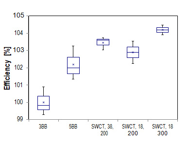
Figure 4: Normalized module power of the mono cells connected with 3 or 5 ribbons, or with SWCT of 38 or 18 wires with 200 μm wire diameter, or with SWCT of 18 wires with 300 μm wire diameter
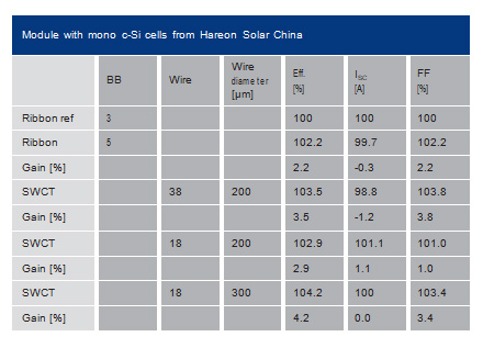
Table 2 collects the data of modules prepared with high temperature mono cells and HJT cells. Using SWCT, mod- ules have a relative FF gain of 3.7% and 5.1% respectively, for the high temperature and HJT solar modules connect- ed with 38 wires compared to the same cells but intercon- nected with ribbons. The electrical loss in cell interconnec- tion is shared by the front and the back side of the solar cell and is proportional to the square value of the current. Thickening the ribbon would reduce the loss in the 3 and 5 ribbons as demonstrated by Qi et al [2]. However, doing this is not desirable, as it requires more encapsulant dur- ing module production, i.e. more cost, and puts the solar cells under greater stress and therefore increases the risk of breakage by a factor 2 [2]. SWCT reduces electrical losses both in the fingers and along the wires. In conclu- sion, SWCT can reduce the electrical loss resulting from the interconnection as shown here and this was also pre- viously reported in the past in [3]. The trade-off between shadowing and electrical loss must always be optimized for each cell design, which is made possible by SWCT for a given cell technology. This study demonstrates that the lower electrical losses of the SWCT compared to a standard 3 ribbon technology can be achieved and is transformed into an efficiency gain of 4.2% and 7.0 %, for diffused and HJT solar module technologies respectively. The gain is higher for the HJT cell compared to the high temperature cell since a low temperature paste is used for the HJT cell. This low temperature paste has a reduced conductivity, and therefore the advantage of SWCT in combination with HJT cells is more pronounced.
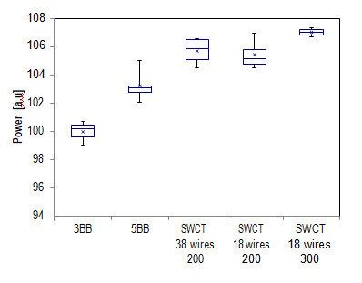
Figure 5: Normalized module power of the HJT cells con- nected with 3 or 5 ribbons, or with SWCT of 38 or 18 wires with 200 μm wire diameter, or with SWCT of 18 wires with 300 μm wire diameter
Table 2: The electrical performance of mono and HJT c-Si solar cells connected with 3 or 5 ribbons or SWCT. The 3 busbar cells are interconnected with ribbon (0.15 mm * 1.5 mm), the 5 busbar with 5 ribbons (0.2 mm * 1 mm) and the busbar-less cells are con- nected with SWCT (wire diameter of 200 μm or 300 μm). The ef- ficiency gain is always compared to the 3BB reference cell.

Optical shading Optical losses in the module are typically the result of light shad- ing, light absorption in inactive layers and light reflection. SWCT reduces shading by avoiding the use of busbars on the cell. Busbar shading is typically 2.9% for a solar cell with 3 busbar design with a 1.5 mm wide busbar. Thanks to the geometry of the round wire used in SWCT, this shading can be reduced to a lower level. This concept was already presented by Braun et al. [4] and it is repro-duced here in Figure 6. The wire geometry allows the light to be reflected either back to the glass, where internal reflection occurs when the angle of incidence is above 42° or directly toward the solar cell. Table 3 collects the IV data of HJT cells without busbars and connected with a varying number of wires in a module. Effective shading of 151 μm for a 200 μm thick wire is found. Here, the effective shading is then 75% of the wire di- ameter. This beneficial effect is the result of the light reflection on the round wire surface, which is then trapped in the module as described in Fig- ure 6. The experimental data also supports the early simulation of Braun et al. [4], which foresaw a shading potential down to 30% for round wire. In conclusion, shading was reduced by 25% compared to ribbon technology, with a potential to be further reduced.
Table 3: Electrical performances of HJT solar cells connected with 6, 18 and 36 wires of 200 μm in diameter. Effective shading diameter is calculated from the linear interpolation of ISC variation with the equation 1 where x is the number of wires, I0 is the ISC without shading, IX the Isc with x wires and d the effective shading diameter.
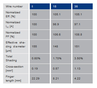
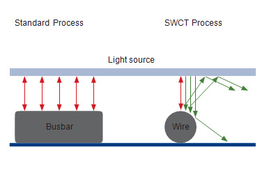
Figure 6: Light reflection on solar module connected with ribbon (left) and wire (right). The round shape of the wire introduces a light trapping effect which reduces the shad- ing of the wire by 25%.
Metallization SWCT improves the cell interconnection by reducing the effective finger length and shading. The potential of SWCT is realized in the direction of combining with new metalliza- tion designs and schemes. Indeed, silver paste consump- tion is a key figure to minimize, in order to reduce the cost of the solar module. 200 mg of silver paste consumption per cell represents 12 g/module and thus 3.7 cts$/Wp for a 300 W module with a silver price of 925 $/kg. This means that production costs can be reduced if busbar printing is avoided and fine lines used or if silver is re- placed with a low cost material.
To achieve this, narrower finger lines or other metalliza- tion schemes are needed and the following experiment illustrates this point. The performance of HJT solar mod- ules made with identical solar cell precursors but using different metallization schemes are presented in Figure 7. These solar cells were either screen printed with three dif- ferent screens or plated with Cu. Screen A was used to print 3 busbars (1.5 mm wide each) and 70 fingers (90- 100 μm wide each) to the front side of HJT cells, i.e. con- suming 350 mg of Ag paste for a 6-inch solar cell. Screen B was used to print 70 fingers only (90-100 μm wide each) to the front side of HJT cells, i.e. 110 mg of Ag paste for a 6-inch solar cell. Screen C was used to print 70 fingers (60-70 μm wide each) to the front side of HJT cells, i.e. 40 mg of Ag paste for a 6-inch solar cell. The fourth design (Option D) for front side metallization used 70 Cu-plated fingers (50-60 μm wide each), i.e. 0 mg of Ag paste for a 6-inch solar cell. Finger resistance was 0.6 Ohm/cm for designs using screen A and B, and 2 Ohm/cm for de- sign using screen C. HJT cells using screen A were con- nected with 3 ribbons and the others interconnected with SWCT. Figure 7 shows that SWCT enabled a reduction in Ag consumption of 21 g/module (350 mg/cell) and a rela- tive increase in module efficiency of 5.7% over the cells with busbars and connected with ribbons. The absence of busbars in screen B, the finer lines of screen C and the fourth design lead to this gain. The effective finger length was shorter due to SWCT and therefore finger power losses were negligible with screen C. In contrast, a three- busbar design combined with 2 Ohm/cm fingers (as used in screen C) would lead to poor cell performance due to a high level of power dissipation in the fingers.
Thanks to SWCT, fine-line printing led to better module performance and constrained on-finger conductivity was relaxed com- pared with conventional ribbon technology. Our simulation indicated that finger resistance up to 100 Ohm/cm could be combined with SWCT without significant power loss- es. In other words, fingers can be made of materials with much lower conductivity than Ag, or they can be made much narrower and/or thinner. This key advantage gives rise to new opportunities for fine line printing technologies, such as aerosol jet printing, ink jet printing, offset printing, as well as plating, dispensing or extrusion.
As presented in the experiment above, fine-line printing and Cu plating improve solar module efficiency and also reduces or eliminates Ag paste consumption. The results presented are for HJT cells here but are also very well adapted to screen printed multicrystalline cell and plated monocrystalline cells. Indeed, Edwards et al [5], reported a gain of 3% in efficiency for a multicrystalline cell with an Ag metallization of only 65 mg compared to a 3 busbar cell connected with ribbons. It was also demonstrated that a plated monocrystalline solar cell with almost no metal, i.e. only 1 μm thick Ni fingers, can achieve FF over 74% at the module level.
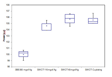
Figure 7: HJT solar cells were screen-printed with three different screens on the cell’s front side. Screen A formed 3 busbars (BB) of 1.5 mm in width and 70 fingers rang- ing from 90-100 μm in width. Screen B formed 70 fingers ranging from 90-100 μm in width and Screen C formed 70 fingers ranging from 50-60 μm in width. Option D formed 70 Cu plated fingers ranging from 50-60 μm in width. The cells metallized with screen A are soldered with ribbon and the other cells were laminated into one cell mini modules with SWCT